This content was translated automatically.
End-to-End Wafer Handling Processes for Greater Efficiency and Precision
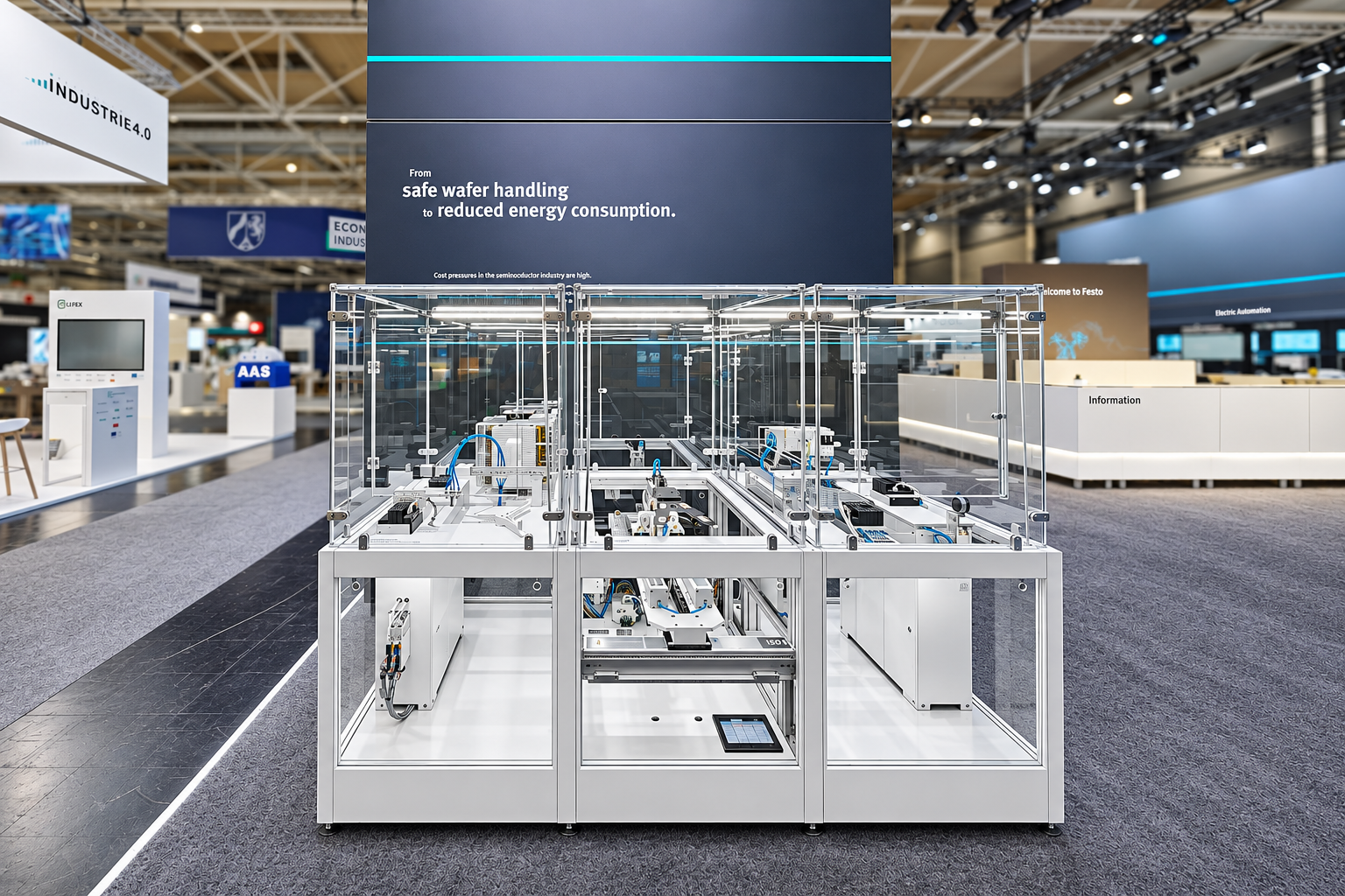
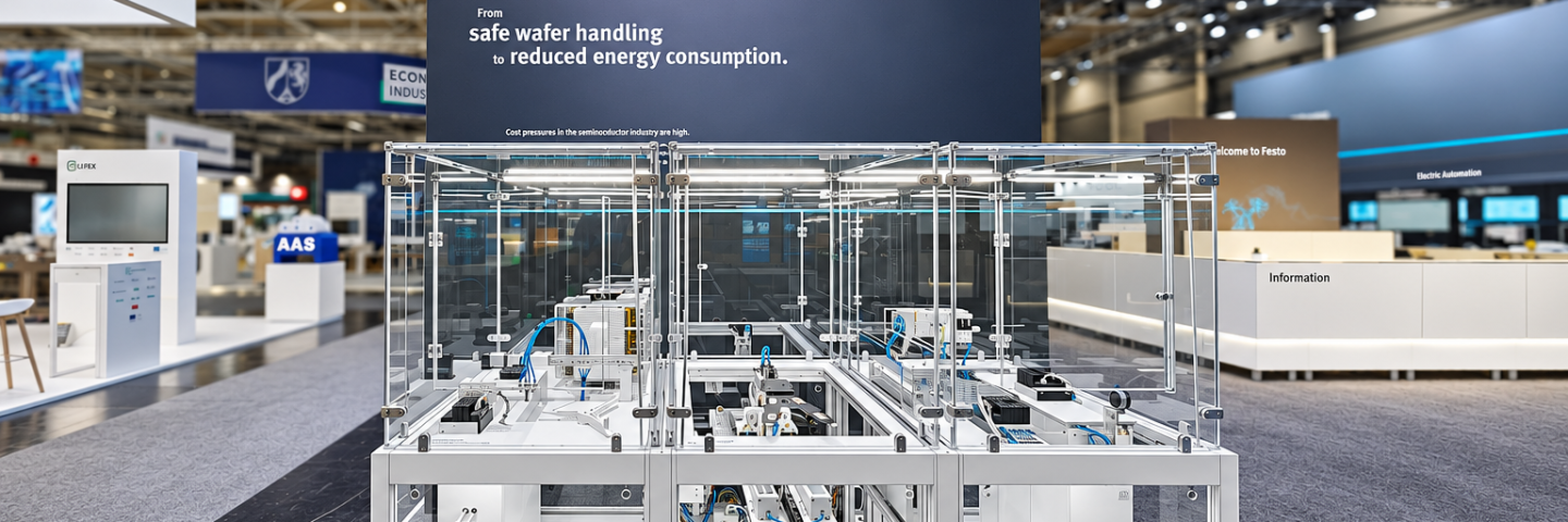
The centerpiece of an exhibit at the Festo booth is a handling cell—the so-called transfer chamber—which simulates a wafer’s path through various process steps. The starting point is an industry-standard transport container for substrates—a so-called FOUP (Front Opening Unified Pod)—from which the wafers are removed.
Here, Festo relies on an inverted gantry system as a cost-effective alternative to traditional SCARA robots. The system enables precise retrieval and transport of the wafers between storage and processing stations.
A particular highlight is the end-effector used, which features an integrated wafer aligner. It combines gripping and positioning in a compact solution. This reduces the required installation space and system complexity while ensuring precise alignment.
Wet chemical processes and coating
Even before removal, a nitrogen purge of the FOUP—using a mass flow controller from Festo—ensures a controlled, low-contamination environment. The wafer is then fed to a coating station. There, an electric linear axis moves a dispensing nozzle precisely over the wafer.
Precision for Vacuum Processes
In a subsequent step, the wafer is transported to a vacuum application, such as that used in dry etching. The system demonstrates how a specialized technology from Festo controls and gently actuates a wafer transfer valve (gate valve) to transfer the wafer into the vacuum chamber with minimal vibration and no particles.
Inside the chamber, a pneumatic pin-lift system lifts the wafer onto a wafer chuck without causing any vibration. After the process, the system lifts the wafer off the chuck again with extreme care and under force monitoring.
A pneumatic micropositioning system positions components such as focus rings with micrometer-level precision. In this way, Festo demonstrates how integrated automation solutions can help increase throughput, process stability, and quality in modern semiconductor manufacturing.
Qualification Required
Festo Didactic offers targeted continuing education programs. The offerings include hands-on training at the plants, the establishment of in-house training facilities, and digital learning content on the Festo Learning Experience (Festo LX)—including topics related to sustainability.
Festo at Semicon Europe in Munich: Hall C1, Booth C1337
Festo is a global player and an independent family-owned company with headquarters in Esslingen am Neckar, Germany. Festo has set standards in industrial automation technology and technical education ever since its establishment, thereby making a contribution to sustainable development of the environment, the economy and society. The company supplies pneumatic and electrical automation technology to 300,000 customers of factory and process automation in over 35 industries. Digitalization, AI and the LifeTech sector with medical technology and laboratory automation are becoming increasingly important. The products and services are available in 176 countries. With about 20,600 employees in over 250 branch offices in around 60 countries worldwide, Festo achieved a turnover of around €3.33 billion in 2025. More than 8% of this turnover is invested in research and development. In this learning company, 1.5 % of turnover is invested in basic and further training. Festo Didactic SE is a leading provider of technical education and training and offers its customers worldwide comprehensive digital and physical learning solutions in the industrial environment.